

Manual
IC test environment
1 IC test system
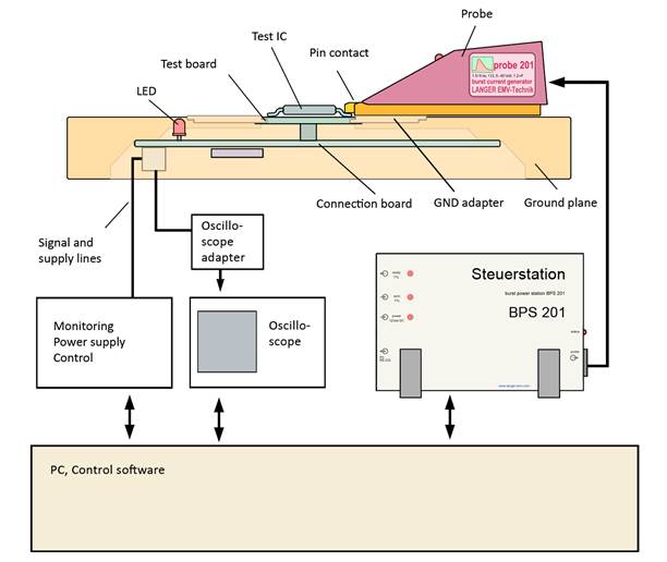
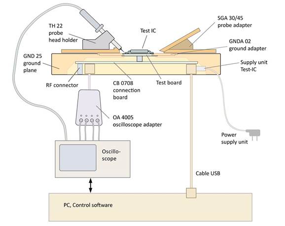
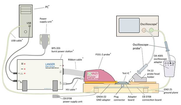
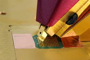
The IC test system can be used to analyse the behaviour of integrated circuits under the selective influence of conducted and radiated disturbances and/or respective emissions.The device under test (integrated circuit) is tested in operation (Figure 1).
The EMC parameters determined with the IC test system allow the user of ICs to:
- Take the IC's EMC parameters into account when the development is planned,
- Adapt the layout design to the IC's EMC parameters,
- Select the ideal IC for the respective application by comparing the EMC parameters of several ICs.
The manufacturers of ICs have the possibility of measuring the EMC parameters of ICs on the one hand and improving the EMC characteristics of ICs during development on the other.
- Pin and field-related measurement of the IC's EMC parameters: voltege (u), current (i), foreward power (pvor), electric field strength (E), magnetic field strength (H)
- Analysis of the causes of immunity problems at weak points in the IC
- Efficient development of ICs in terms of EMC
Advantages of measurements carried out with the IC test system:
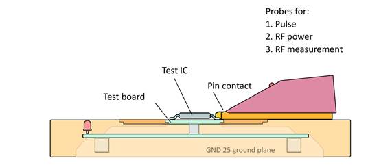
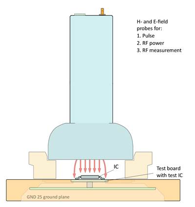
The test IC is located and wired on a universal test board. The test board with the test IC can be used for all of the measurements carried out with the IC test system. Only one circuit board (test board) has to be developed for the test IC.The test IC is arranged on the test board so that all pins of the test IC can be contacted with the probes in conducted EMC tests.The same ICE1 IC test environment can be used for both conducted and all radiated measurements.
ICE1 IC test environment
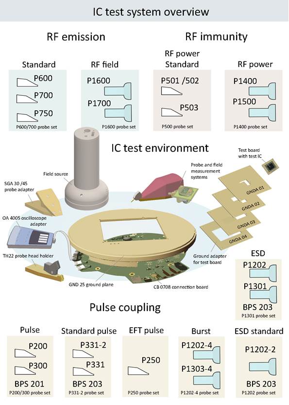
Apart from the probe set (www.langer-emv.de), the following basic components are required for the test set-up:
| Components to fix the test ICs (test fixtures): | Accessories to test the test IC: |
|---|---|
|
|
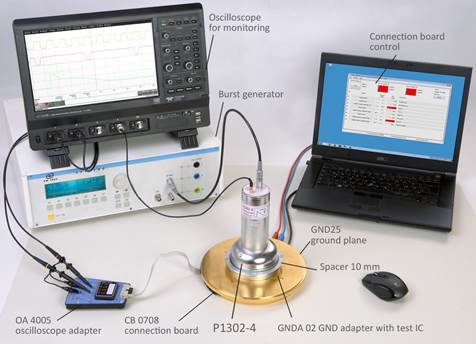
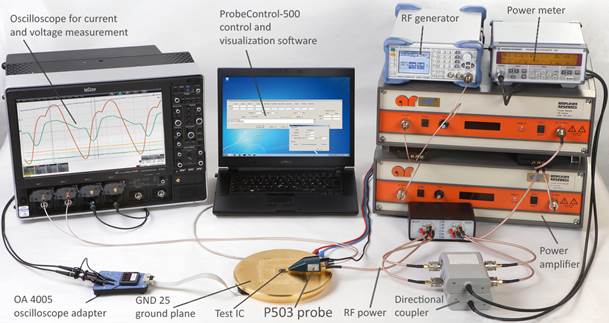
Apart from the IC test system components (ICE1 IC test environment with probe set) the following additional devices may be required for the test set-up depending on the measurement task (Figure 5)(the additional devices are not included in the scope of delivery):
- Disturbance generator (e.g. EFT/burst)
- Oscilloscope
- Spectrum analyzer
- PC
- Power amplifier, frequency generator, directional coupler, etc.
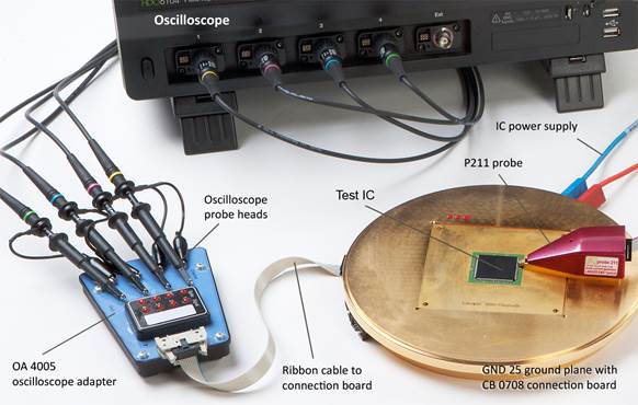
The IC under test is located on a test board in the measurement set-up. Filtered connections link the test board to the connection board located below this. The connection board in turn connects the device under test to the PC. The IC can be controlled and monitored with the enclosed software. The connection board is on the bottom of the ground plane which forms a fixed ground reference system for the measurement. The probes are placed on to the ground plane and used to inject disturbances into the test IC by conductive or capacitive/inductive coupling or to measure its emissions.
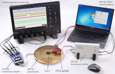
The probes are connected either to an external device (spectrum analyzer or disturbance generator) or to the BPS burst power station from Langer-EMV to carry out the respective measurement.
The burst power station is included as an accessory with certain probes. The probe's pulse voltage, pulse frequency and polarity can be controlled with the enclosed BPS-Client control software. The injected disturbance pulse can thus be defined precisely and reproduced at any time.
 | Conducted coupling |
 | Capacitive / inductive coupling |
| | |
2 ICE1 IC test environment: components
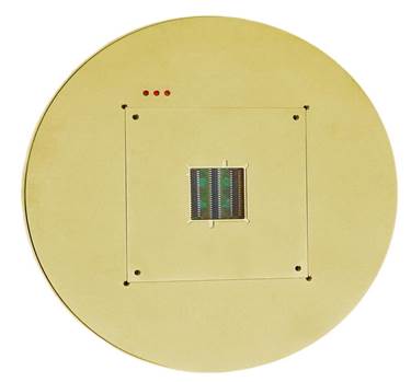
2.1 Test board
The test IC is mounted on the test board. The test board is the interface between the IC and the IC test system (Figure 7). The size of the test board depends on the size of the test IC and the recesses of the GND adapter.
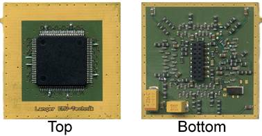
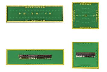
A special test board has to be developed and manufactured for each test IC (different pinout and function).
The customers can either do this themselves on the basis of the Guide line IC EFT immunity from Langer EMV-Technik GmbH or the test board can be developed and manufactured on the basis of the customer's specifications by Langer EMV-Technik GmbH.
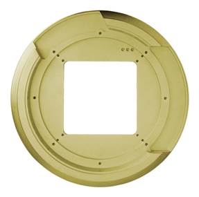
2.2 GNDA ground adapter
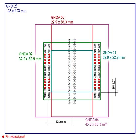
The GNDA 01 to 04 ground adapter is inserted into the respective opening of the GND 25 ground plane. There are four different recess options for the test board. The size of the test board and thus the selection of the ground adapter depend on the dimensions of the IC to be tested.
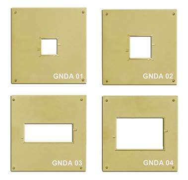
Figure 10 shows the four different recesses of the ground adapters. Only certain pins of the 56-pole connector can be used to connect the connection board to the test board depending on the recess. A TEM cell print 100 x 100 mm can be inserted into the GND 25 ground plane (Figure 10) instead of the ground adapter.
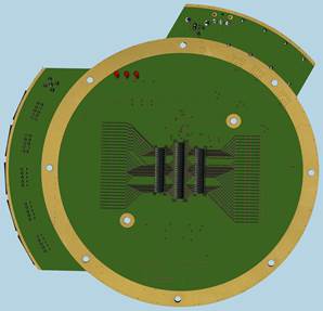
2.3 GND 25 ground plane
The GND 25 ground plane is made of steel and has a gold-plated surface. The probes are fixed on the ground plane with magnets. The steel material allows the probes to adhere magnetically to the surface and the gold plating allows them to make contact in compliance with RF requirements. The 103x103 mm recess is provided for the insertion of:
- 1. GNDA 01-04 ground adapters and
- 2. TEM cell print 100x100 mm.
The CB 0708 connection board is mounted on the bottom of the ground plane. The ground plane has three openings for the LEDs of the connection board (Figure 11 and Figure 12).
Figure 11: Top and bottom of the GND 25 ground plane
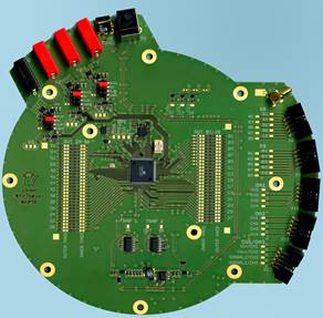
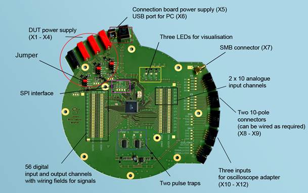
2.4 CB 0708 connection board
The CB 0708 connection board is the core component of the ICE1 IC test environment. It is fixed to the GND 25 ground plane with 10 Phillips screws.
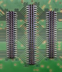
The CB 0708 connection board is responsible for controlling and monitoring the test IC. It is connected to the test board and thus to the test IC via a connector (Figure 19). A 56-pole connector and two 44-pole connectors connected in parallel are located on the top of the connection board (Figure 13) to hold the test board. The three LEDs are used to visualize freely selectable signals.
The microcontroller in the middle on the bottom (Figure 14) controls the communication with the test IC. It also provides an interface to the PC for transmitting and receiving commands and signals via USB.
Sockets for the connection of external devices and signals are located at the edge of the connection board. The incoming and outgoing signals can be connected to the DUT and microcontroller via the board's wiring fields.
2.4.1 Interfaces of the connection board
External interfaces
| Plug designation | Type | Use |
|---|---|---|
| X1 | Lab socket | Ground of the DUT power supply |
| X2 | Lab socket | DUT power supply |
| X3 | Lab socket | DUT power supply |
| X4 | Lab socket | DUT power supply |
| X5 | Low voltage socket | 12 V power supply for the connection board (as an alternative to the USB power supply) |
| X6 | USB socketType B | Power supply for the connection board, connection of the connection board to the PC |
| X7 | SMB plug | Input signals such as a clock generator |
| X8 | 2.54 mm socket, 2*5-pole | Input/Output of signals |
| X9 | 2.54 mm socket, 2*5-pole | Input/Output of signals |
| X10 | 2.54 mm socket, 2*5-pole | OA4005 oscilloscope adapter |
| X11 | 2.54 mm socket, 2*5-pole | OA4005 oscilloscope adapter |
| X12 | 2.54 mm socket, 2*5-pole | OA4005 oscilloscope adapter |
| X13 | 1.27 mm socket, 2*28-pole | Stecker für die Testleiterkarte auf Vorderseite des CB 0708 |
| X14 | 1.27 mm socket, 2*22-pole | Stecker für die Testleiterkarte auf Vorderseite des CB 0708 |
| X15 (SPI) | 1.27 mm socket, 2*3-pole | SPI (serial peripheral interface) for control and monitoring tasks |
| X16 | 1.27 mm socket, 2*22-pole | Connector for the test board on the top of the CB 0708 |
Interfaces of internal functional blocks
| INNER PADS 01-56 | 56 pads for digital input and output channels of the microcontroller freely programmable 01 to 10: pads for analogue input channels; an optional voltage divider can be added |
| OUTER PADS 01-56 | 56 pads to the connector (top side) for the test board |
| Pads between INNER and OUTER pads | 56 custom-wireable filters |
| SPI | 4 pads for the SPI port that can be wired with the test IC for control and monitoring tasks |
| V1 to V3 | Pads for three outputs for the DUT power supply (3-24 V, 500 mA)
|
| TRAP1, TRAP2 2xIN, 1xOUT | Pads for two pulse traps (pulse stretching)
|
| X8.01 bis X8.10 X9.01 bis X9.10 | Pads for two 10-pole connectors X8, X9 for use as required |
| OA1 CH 1 - CH 4 OA2 CH 1 - CH 4 | Pads for two connectors for OA 4005 4-channel oscilloscope adapter |
| CU1/OA3 CH 1 - CH 4 | Pads for connector either for another OA 4005 4-channel oscilloscope adapter or a control unit (CU1) |
| Pad of X7 | SMB RF socket for connecting a clock generator, etc. |
| LED1 to LED3 | Pads for monitoring LEDs |
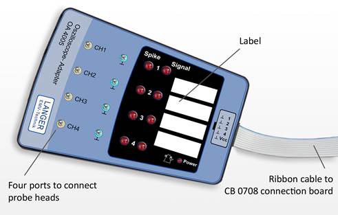
2.5 OA 4005 oscilloscope adapter
The oscilloscope adapter is a visualisation device for signals of the test IC. It is connected to the CB 0708 connection board (X10 to X12 (Figure 16) for three oscilloscope adapters) via the ribbon cable (Figure 16).
The Signal 1-4 and Spike 1-4 LEDs visualize the signals of the test IC. CH1 to CH4 are four ports where oscilloscope probe heads can be connected. The OA 4005 is supplied with power from the connection board via the ribbon cable.
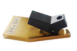
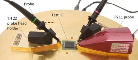
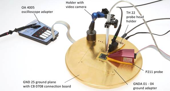
2.6 TH 22 probe head holder
The probe head holder is used to accommodate the oscilloscope probe heads and ensures that the probe tip makes reliable contact with the test IC. Magnets that are contained in the bottom of the probe head holder ensure that it adheres to the GND 25 ground plane and is fixed in place.
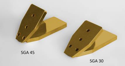
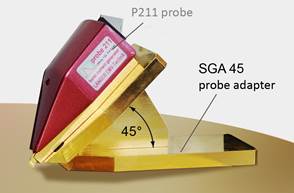
2.7 SGA 30 and SGA 45 probe adapters
These probe adapters are used to position the probe at an optional angle of 30° (SGA 30) or 45° (SGA 45) (Figure 18).
Magnets that are contained in the bottom of the probe adapter ensure that it adheres to the GND 25 ground plane and is fixed in place.
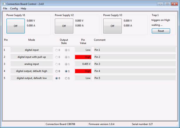
2.8 Connection board control software
The connection board control software is used to monitor the test IC. The test IC is monitored by the microcontroller of the CB 0708 connection board. The signals are transmitted to the connection board control software via a USB connection and displayed on the user interface.
3 System set-up
The ground plane is usually delivered with the connection board inserted.
The ICE1 IC test environment allows the user to implement a wide variety of measurement set-ups in connection with the probe sets. The respective measurement set-up depends on the customer's test objective. The ICE1 components, the probe set and external devices have to be selected according to this test objective
3.1 ICE1 IC test environment: the test IC is embedded in the user's electronic device
The test IC is embedded in the user's electronic device as a test environment. The user's electronic device is used to control, monitor and support the test IC functions and replaces the connection board of the ICE1 IC test environment. The test IC is operated via the user's electronic device instead of the connection board. The connection board is removed from the GND 25 in this case. The test board with the test IC is inserted into the GNDA ground adapter and GND 25 ground plane. The user's electronic device is connected to the bottom of the GND 25 via an adapter plug. The following components can be used for this test set-up: SGA 30 and SGA 45 probe adapters as well as the TH 22 probe head holder.
3.2 ICE1 IC test environment: connection board without a PC
The test IC is operated with the connection board. The connection board is responsible for controlling the test IC (via a control unit that is not included in the scope of delivery, X12 - Figure 15) and monitoring the test IC (three LEDs, Trap2 and oscilloscope adapter). The test board with the test IC is inserted into the ground adapter and GND 25 ground plane. The wiring fields of the connection board are hard-wire programmed via soldered connections (e.g. enamelled copper wire) depending on the test objective.
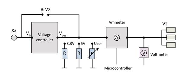
The power supply unit is connected to the connection board. An external power supply (X1 to X4) supplies power to the test IC. X1 is the ground (GND). The external voltages V1 to V3 can be connected to X2 to X4. The connection board is equipped with three voltage controllers. The voltage of the voltage controllers can be set with jumpers to 3.3 V, 5 V or freely selected (with a divider). In addition, the input voltage that is present at the sockets X2 to X4 can be connected to the outputs V1 to V3 via the wiring links BrV1 to BrV3 and a bypass (jumper). The outputs of the voltage controllers V1 to V3 are connected to the selected pads of the wiring fields with wire. These pads are connected to the power supply of the test IC.
The following components can be used for this test set-up: SGA 30 and SGH 45 probe adapters, the OA 4005 oscilloscope adapter as well as the TH 22 probe head holder.
External devices such as a spectrum analyzer, oscilloscope, frequency generator, disturbance generator, etc. can be operated in the ICE1 IC test environment (Figure 20 , Figure 21). These devices can be connected to the following components:
- TH 22 probe head holder
- OA 4005 oscilloscope adapter
- Measurement outputs of the probes (user manual of the respective probe set)
- Test parameter inputs of the probes (user manual of the respective probe set)
- RF socket X7 on the CB 0708 connection board (Figure 15).
3.3 ICE1 IC test environment: connection board with a PC
The test IC is operated with the connection board (Figure 19). The connection board is responsible for controlling and monitoring the test IC. The test board with the test IC is inserted into the GNDA GND adapter and GND 25 ground plane. The wiring fields of the connection board are hard-wire programmed via soldered connections (e.g. enamelled copper wire) depending on the test objective.
A USB connection is then established to the PC which ensures the power supply to the connection board.
The device under test is connected as described in chapter 3.2.
The following components can be used for this test set-up: SGA 30 and SGH 45 probe adapters, the OA 4005 oscilloscope adapter as well as the TH 22 probe head holder.
External devices such as a spectrum analyzer, oscilloscope, frequency generator, disturbance generator, etc. can be operated in the ICE1 IC test environment (Figure 20 and Figure 21). These devices can be connected to the following components:
- TH 22 probe head holder
- OA 4005 oscilloscope adapter
- Measurement outputs of the probes (user manual of the respective probe set)
- Test parameter inputs of the probes (user manual of the respective probe set)
- RF socket X7 on the CB 0708 connection board (Figure 15).

3.4 OA 4005 oscilloscope adapter in the test set-up
The oscilloscope adapter can be used within the connection board system set-up with or without a PC being connected (chapters 3.2 and 3.3). The oscilloscope adapter is connected to the sockets X10 to X12 of the CB 0708 connection board via the ribbon cable (Figure 15: Functional blocks of the connection board).
CH1 to CH4 are four ports where the oscilloscope probe heads are connected to ground or signal (Figure 22). A total of three oscilloscope adapters can be connected to the connection board in the ICE1 IC test environment
3.5 TH 22 probe head holder in the test set-up
The TH 22 probe head holder is placed on to the GND 25 ground plane. It is fixed in place on the ground plane by internal magnets. An oscilloscope probe head is inserted into the probe head holder. The probe head's ground connection cable may have to be removed under certain circumstances. The user must make sure that there is a good ground connection between the probe head and probe head holder.
The probe head holder has to be adjusted on the GND 25 to contact a pin of the test IC with the tip of the probe head.
4 ICE1 IC environment: mode of operation
The components of the IC test system and external devices are selected and set up (chapter 3) depending on the test IC and measurement objective.
The CB 0708 connection board is then programmed and the selected test IC signals to be monitored are linked to the fault detectors and respective ports of the connection board (->Guide line IC EFT immunity).
4.1 ICE1 IC test environment: connection board without a PC
The connection board is not connected to the USB interface (X6 - Figure 15) of the PCs in this mode of operation. Power is supplied via the external 12 V power supply unit (connection board power supply X5 - Figure 15) for the whole connection board.
Three monitoring LEDs allow the user to monitor the test IC easily and directly.In addition, the test IC can be controlled and monitored with external devices via the sockets X7 to X12 (Figure 15). The SGA 30 and SGA 45 probe adapters, the TH 22 probe head holder with the respective measuring devices and the OA 4005 oscilloscope adapter can be used for monitoring purposes.
4.2 ICE1 IC test environment: connection board with a PC
The CB 0708 is controlled and monitored by a microcontroller and connected to a PC via USB. Power is supplied to the connection board directly via the USB port or additionally by an external 12 V power supply unit connected to socket X5. Power for the test IC is supplied separately via the 4 mm sockets X1 to X4 from an external power supply. The power supply for the test IC can thus be monitored individually.
The connection board components can be connected to each other (programmed) with enamelled copper wire via soldering pads to suit the user's needs. The IC signals can thus be connected to the following positions (->Guide line IC EFT immunity):
- Microcontroller (DUT 01-28 and 29-56)
- 10-pole connector X8 - X12
- RF socket X7
- Pulse traps Trap1 and Trap2
- LEDs 1 to 3
- Power supplies V1 - V3.
4.3 Mode of operation and programming of the CB 0708 connection board
Figure 15 shows the connection board's functional blocks.
4.3.1 Power supply of the test IC
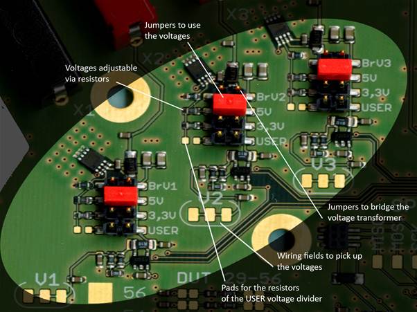
There are three separate inputs, namely V1 to V3 (X1 to X4), for the DUT's power supply. A voltage controller regulates the input voltage to the desired output voltage (Vin >= Vout+1 V up to max. 24 V). The output voltage can be smoothly adjusted with the USER jumper and a potentiometer-type resistor. There are three jumper connection options for each input voltage to adjust the output voltage (Figure 24):
- 5 V: output voltage 5 V
- 3.3 V: output voltage 3.3 V
- User: the output voltage is adjusted via a resistor R which can be soldered in place.
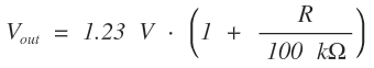
The USER voltage is calculated with the following equation:
The resistor R is soldered on to the pads to the left of the USER slot (Figure 24). The jumper has to be plugged in the respective place of the two-row connector to use one of the voltages. The jumper has to be plugged in BrV1 to BrV3 if the external voltage present on sockets X2 to X4 is to be directly applied to the test IC.
Only one jumper may be plugged in each of the two-row plug connectors.
Attention: if no jumper is plugged in, the output voltage is equal to the respective input voltage of the voltage transformer.
The voltage for hard-wire programming is tapped from the "wiring fields to tap the voltages" (Figure 24).
The voltage and current are measured on the outputs of voltage controllers V1 to V3. The measured values are transmitted to the microcontroller. Figure 25 shows the power supply circuit, taking voltage V2 as an example.
The voltage selected for the test IC is hard-wire programmed. A wiring link is soldered from V1 to V3 to the respective pad of the DUT 01-56 wiring field (Figure 15).
4.3.2 Connection board power supply
The connection board is supplied with power from the PC via the USB cable. It can also be supplied with 12 V by a power supply unit via socket X6.
4.3.3 LEDs
Three custom-wireable LEDs are available to monitor the test IC.The circuit for monitoring the test IC with the LEDs can be designed on the basis of the Guide line IC EFT immunity.
4.3.4 Wiring fields for test IC signals
The OUTER PADS wiring fields: DUT 01- 56 (Figure 15) are connected to the plug on the top side of the connection board. The test board with the test IC is inserted into this plug. The INNER PADS wiring fields: DUT 01- 56 (Figure 15) are connected to the microcontroller of the connection board. The test IC is connected to the microcontroller via wiring links between INNER and OUTER PADS. This connection can also be implemented via filters that are located between the INNER and OUTER PADS.
The wiring fields allow the connection of the test IC and microcontrollers respectively to internal (TRAP 1, TRAP 2, LED 1 to 3, SPI) and external components (X7 – X12). The microcontroller ports can be programmed as inputs or outputs depending on the test IC signal connected.
4.3.5 Filter wiring
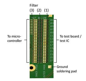
The test IC signals are fed to the microcontroller via filters.
| Filter (1) | 100 pF at the OUTER PADS to ground |
| Filter (2) | Chip-Ferrit 2,5 kΩ @100 chip ferrite + 10 kΩ resistor to the inputs of the microcontroller (filter + level shifter) |
| Filter (3) | the analogue ports 1-10 have got an additional optional input voltage divider. The pads (3) that are bare on delivery can be fitted with a resistor. |
They form a voltage divider together with the 10 kΩ resistor of the filter (2). The maximum voltage of the analogue inputs is limited to 2.5 V by the internal reference.
The values of the filter (3) have to be matched so that 2.5 V are not exceeded!
The filters are already connected to the OUTER PADS (test IC) and the INNER PADS (microcontroller) on the other side on delivery. The connection to the filtered can be disconnected between the pair of soldering pads (Figure 26: Arrangement of the filters (1 to 3) on the INNER PADS and OUTER PADS ).The four ground soldering pads are used for wiring to ground (Figure 26).
4.3.6 Test board connection options on the top of the CB 0708
The test board may have connectors in two different areas on the bottom of it.
- lengthwise in the middle
- lengthwise on the outer edges
Both options are provided for on the top of the CB 0708 connection board (Figure 27) to plug in the test board.

4.3.7 Pulse traps
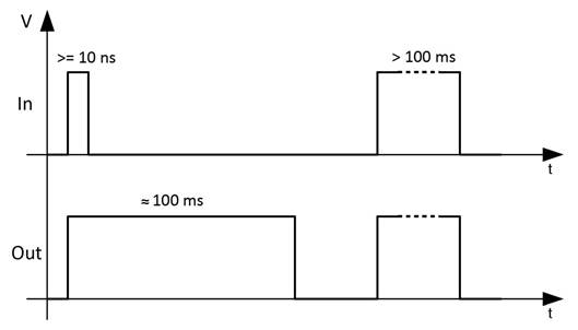
The test IC can output error signals of less than 1 ms. These signals would be imperceptible if an LED is used to indicate them. The pulse traps stretch these short pulses to 100 ms. Short individual pulses with a pulse width of approx. 10 ns can thus be detected and visualised. The input and output voltage is 5 V (Figure 28). The pulse traps are also used to stretch the signals for reading them into the microcontroller ports.
Trap 1: custom-wireable input; the pulse trap is read out and reset via the software.
Trap 2: custom-wireable input and output; the output can be directly connected to the LED, for example, fixed pulse duration can be stretched to 100 ms.
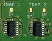
Figure 29 shows the timing diagram for trap 2. Pulses with a pulse width of more than 10 ns are stretched to 100 ms. Pulses with a pulse width of more than 100 ms remain unchanged.
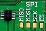
4.3.8 SPI
The SPI port on the connection board is available (Figure 30) if the test IC is to be monitored and controlled via SPI. The SPI signals have to be wired to the test IC via the respective filters and OUTER PADS.
4.3.9 Connectors
There are five 2x 5, RM 2.54 mm connectors (X8 to X12) on the connection board. Please refer to Figure 31 for the pin numbers. External components can be linked via these connectors, such as: OA 4005 oscilloscope adapter, control unit or the customer's own devices used to monitor and control the test IC.
| X8 and X9 | 10 custom-wireable pins |
| X10 to X12 | X10 to X12: Pins 2, 4, 6, 8 are custom-wireable. Pins 1, 3, 5, 7, 9 are assigned to the ground. The 5 V power supply of the connection board is available on pin 10 for the operation of external components. |
4.3.10 RF socket
The RF socket (X7) is used to transmit RF signals to the test IC (Figure 15). A test IC can be supplied with a certain external clock rate via this socket (signal generator, etc.), for example. Furthermore, signals with a higher bandwidth as implemented by the oscilloscope adapter can be transmitted from the test IC.
4.4 Mode of operation of the OA 4005 oscilloscope adapter
The oscilloscope adapter is used to connect a 4-channel oscilloscope to the connection board to produce an oscillogram of signals from the test IC (reset, Chipselect (CS), etc.). The test IC signals are led to the OUTER PINS on the connection board via the test board and connector and from there to the soldering pads (CH1 to CH4) of sockets X10 to X12 via the filters. The signal path then continues to the oscilloscope adapter via the ribbon cable.
The oscilloscope adapter has two functions:
- to transmit signals from the test IC to the oscilloscope probe heads
- to indicate the signals on the LEDs of the oscilloscope adapter
Regarding 1. The signals of the test IC are fed to the connection pins for the probe heads – signal CH1 to CH4 in the oscilloscope adapter via a low pass (1 k, 22 pF). The low pass has a bandwidth of 7 MHz. It is used to keep high-frequency test signals away from the oscilloscope. The high-frequency test signals are injected into the test IC with the probes during the test, especially if the P500 probe is used to inject RF into the test IC. The high frequency would be superimposed on the signal of the test IC and could lead to the alias effect in the oscilloscope. The low pass blocks all RF above 7 MHz and prevents the alias effect in the oscilloscope.
Regarding 2. The signals of the test IC are fed to the display LEDs. The LED signal indicates the high – low state of the original signal. A pulse trap is connected in the incoming circuit of the Spike LED. The Spike LED indicates short, otherwise imperceptible signals, stretched to 50 ms The LEDs offer a simple possibility of monitoring the test IC during a test. Incomplete resets whose duration is in the ns range can be triggered in the test IC, for example. These resets become visible on the Spike LED.
The oscilloscope adapter can also be operated without an oscilloscope. The LED display facilitates monitoring of the test IC.
4.5 Mode of operation of the TH 22 probe head holder
The probe head holder is used to accommodate an oscilloscope probe head. The probe head holder with the respective oscilloscope probe head fitted allows measurements of up to approx. 1 GHz.
4.6 Mode of operation of the SGA 30 or SGA 45 probe adapter
BGA ICs have no pins that are accessible for the probe. Therefore a pad grid that corresponds to the BGA's pinout is arranged under the BGA circuit on the other side of the test board.
The probe adapter allows the user to contact this pad grid on the test board. The probe can be positioned on the pads to be contacted with the probe adapter from above in an inclined position at an angle of 30° or 45°. The probe tip can thus access hard-to-reach locations adjacent to or even on the test board.
The probe adapter is fixed on the GND 25 ground plane with internal magnets.
5 Software
5.1 Installation requirements
- Pentium III with at least 500 MHz
- 128 MB RAM
- 20 MB hard drive memory
- USB interface
- Windows XP with SP3 or later
5.2 Installation
5.2.1 Installation instructions
Insert the connection board installation CD into the CD-ROM drive of your PC. First install the driver ‘CDM20828_Setup.exe’ from the ‘Driver’ subdirectory on the installation CD. Second install the application ‘Connection Board Control.exe’ from the installation CD. Third connect the connection board to your PC.
5.2.2 Testing the installation
Make sure that the connection board is connected to your PC. Click on Connection Board Control in the Windows start menu under Connection Board Control. The main Connection Board Control screen opens (Figure 35). The connection board with its firmware version and serial number is displayed in the status bar. The installation is now complete.
5.3 Using the Connection Board Control software
Start Connection Board Control by clicking on the respective start menu option in the Programme folder -> Connection Board Control. The connection to the Connection Board is established automatically.
5.3.1 Menu
| File → Quit | - Quits the Connection Board Control software |
| Config → Load Settings ... | - Loads pin settings that have been stored beforehand |
| Config → Settings | - Opens the Pin Settings dialogue |
| Config → Save settings | - Stores the current pin settings |
| Config → Save settings as ... | - Saves the current pin settings under a new name |
| Help → Help | - Opens this user manual |
| Help → About | - Software version information |
5.3.2 Pin Settings dialogue
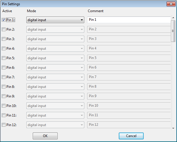
The Pin Settings dialogue (Figure 36) can be opened via the Config -> Settings menu. The Pin Settings dialog allows the user to activate pins (active), set the mode of operation (mode) and enter comments (comment).
Five modes of operation are available under mode.
| digital input | - digital input pin without pull-up resistor |
| digital input with pull-up | - digital input pin with pull-up resistor |
| digital output, default: low | - digital output pin; Low is the start value |
| digital output, default: high | - digital output pin; High is the start value |
| analog input | - analogue input pin (only possible with the pins provided for this purpose) |
| Tabele 1 Modes of operation | |
Deactivated pins remain in the digital input mode on the connection board.
The pin settings can be stored in a file via Config -> Save settings. Connection Board Control must be connected to the connection board to be able to load the file subsequently via Config -> Load settings.
5.3.3 Power supply of the test IC
The control panels for controlling and measuring the test IC power supplies are located on the user interface of the Connection Board Control software (Figure 35). The power supplies are designated Power Supply V1-V3. The button switches the associated test IC power supply on and off. The voltage and current input of the test IC is displayed to the right of each button.
5.3.4 Trap 1
The Trap 1 pulse trap of the connection board monitors static signals of the test IC for short-time errors. The high or low basic state of the signal defines the signal state of the pulse trap. The pulse trap is triggered by an error-related signal change. It can be reset to the basic state of the signal by pressing the Reset button on the user interface.
The signals from the Trap 1 pulse trap of the connection board are transmitted to the user interface of the software. The corresponding display and control elements can be accessed via Trap 1 on the user interface. The colour of the Reset button shows the state of the pulse trap. The colour of the button is grey in the untriggered state, it turns to red if a signal change triggers the pulse trap. Triggers on High/Low signals the state in which the pulse trap is triggered the next time. The pulse trap is reset by pressing the Reset button. It is triggered again by the next trigger event.
5.3.5 Display of the test IC pin signals
The test IC pin signal display is located under the Power Supply and Trap 1 display.
| Pin | Number of the pins (corresponding to INNER PADS Connection Board 01-56, set in the Pin Settings dialogue Figure 36) Figura 36) |
| Mode | Display of the set mode of operation (Tabele 1: Modes of operation)) |
| Output State | Display of the state of the INNER PADS outputs (microcontroller of the connection board) 0 or 1 (configuration in the Pin Settings mode dialogue, Table 1: Modes of operation) |
| Pin Value | Current output value, high, low, Voltage, Current |
| Comment | Comment feature for the user |
5.3.6 Status bar
The status bar at the bottom of the window shows from the left to the right: Manufacturer of the connection board, detailed board designation, board firmware version, board serial number of the connection board.
5.3.7 Remote control commands for the Connection Board
The connection board features can be accessed via the USB interface of the connection board. A variety of control commands are available which can be integrated into the software from a library. You can thus write your own application in C/C++ to control the connection board or integrate it into other processes.
- Setting/evaluating the I/O ports
- Configuring interrupts
- Measuring the voltage/current of V1-V3
- Setting/evaluating the Trap 1 pulse trap
- Configuring the SPI interface
The control commands are listed and documented below and in the file ‘cb0706.h’ in the ‘lib’ subdirectory of the installation CD.
Contact: software@langer-emv.de
General remarks
- For all the functions: negative return values indicate an error.
- Get the error description with cb_get_error_msg().
- Low pin state is represented by 0, high pin state by 1.
- Input pin direction is represented by 0, output pin direction by 1.
- False is 0, true is 1.
- The digital pin numbers start with 1, not 0.
- Power supply numbers go from 1 to 3.
int cb_open()
Call this before use.
int cb_close()
Call this after use (enables others to call cb_open()).
int cb_is_connected()
Check wether the ConnectionBoard is connected.
int cb_company(char* value, int size)
Get manufacturer name of device. value must be a pointer to allocated buffer of given size.
int cb_device(char* value, int size)
Get device name. value must be a pointer to allocated buffer of given size.
int cb_firmware_version(char* value, int size)
Get firmware version of device. value must be a pointer to allocated buffer of given size.
int cb_serial_number(char* value, int size)
Get serial number of device. value must be a pointer to allocated buffer of given size.
int cb_get_digital_pin_count()
Returns the total number of pins on the board.
int cb_get_analog_pin_count()
Returns the number of adc pins on the board.
int cb_get_pin_states(int* digital_pins, int ndigital, double* analog_pins, int nanalog)
Get the pin states. digital_pins and analog_pins must be large enough to store all the pins.Size of the arrays must be at least cb_get_pin_count() for digital_pins and 16 for analog_pins.ndigital and nanalog are the number of elements in the arrays.
- analog_pins[0]: voltage power supply 1
- analog_pins[1]: current power supply 1
- analog_pins[2]: voltage power supply 2
- analog_pins[3]: current power supply 2
- analog_pins[4]: voltage power supply 3
- analog_pins[5]: current power supply 3
- analog_pins[6-15]: voltage at pins 2-11 (CB 0706), pins 1-10 (CB 0708)
bool* cb_get_digital_buffer()
double* cb_get_analog_buffer()
Get pointer to the buffer where pin values are stored. It will (and may) never be destroyed.
int cb_set_pin_adc(int pin, int state)
Make a pin an adc pin. See cb_has_pin_adc() to check if a certain pin has adc support.
int cb_get_pin_adc(int pin)
int cb_has_pin_adc(int pin)
Check if pin is/can be configured as adc pin.
int cb_set_pin_direction(int pin, int dir)
int cb_get_pin_direction(int pin)
Set/get the pin direction. 0 = input, 1 = output
int cb_get_pin_input(int pin)
Get the input value of the pin. 0 = low, 1 = high
int cb_set_pin_output(int pin, int output)
int cb_get_pin_output(int pin)
Set/get the output of a pin. 0 = low, 1 = high
int cb_set_pin_pullup(int pin, int pullup)
int cb_get_pin_pullup(int pin)
Enable/disable the pull up resistance for a pin.
int cb_reset_trap()
Reset the trap.
int cb_is_trap_triggered()
Check if trap was triggered.
int cb_get_trap_trigger_value()
Get the value on which the trap will trigger. 0 = low, 1 = high
int cb_get_trap_input()
Get the trap input value.
int cb_enable_ps(int ps, int state)
Enable/disable a certain power supply.
int cb_is_ps_enabled(int ps)
Check if a power supply is enabled.
int cb_get_ps_voltage(int ps, double *pvoltage)
Get the voltage in Volt from a power supply.
int cb_get_ps_current(int ps, double *pcurrent)
Get the current in Ampere from a power supply.
const charcb_get_error_msg()
Get the error message for the last error.
6 Safety instructions
When using a product from LANGER EMV Technik GmbH, please observe the following safety instructions to protect yourself from electric shocks or the risk of injuries. The device may only be used by personnel who are qualified in the field of EMC and who are fit to work under the influence of disturbance voltages and (electric and magnetic) burst fields. Read and follow the operating instructions and keep them in a safe place for later consultation.
- Never use any damaged or defective devices.
- Carry out a visual check before using a measurement set-up with a Langer EMV-Technik GmbH product. Replace any damaged connecting cables before starting the product.
- Never leave a Langer EMV-Technik GmbH product unattended whilst this is in operation.
- The Langer EMV-Technik GmbH product may only be used for its intended purpose. Any other use is prohibited.
- Observe the operating and safety instructions for all devices used in the set-up.
- People with a pace-maker are not permitted to work with this device.
- The test set-up should always be operated via a filtered power supply.
- Attention! Functional near fields and interference emissions may occur when operating EMC test set-ups. The user is responsible for taking measures to prevent any interference to the correct function of products outside the EMC environment of the test set-up (in particular through radiated interference).
This can be achieved by:- Observing an appropriate safety distance,
- Use of shielded or shielding rooms.
- The disturbances that are injected into the ICs can destroy (latch-up) the device under test if their intensity is too high. Protect the device under test by:
- increasing the disturbance gradually and stopping when a functional fault occurs,
- interrupting the power supply to the device under test in the event of a latch-up.
Attention! Make sure that internal functional faults are visible from outside. The device under test may be destroyed due to an increase in the injection intensity if the faults are not visible outside. Take the following measures as necessary:
- monitoring of representative signals in the device under test,
- special test software,
- visible reaction of the device under test to inputs (reaction test of the device under test).
We cannot assume any liability for the destruction of devices under test!
7 Warranty
Langer EMV-Technik GmbH will remedy any fault due to defective material or defective manufacture, either by repair or by delivery of replacement, during the statutory warranty period.
This warranty is only granted on condition that:
- the information and instructions in the user manual have been observed.
The warranty will be forfeited if:
- an unauthorized repair is performed on the product,
- the product is modified,
- the product is not used according to its intended purpose.