

The weak points for the susceptibility to interference in modern electronics often lie in the circuits (ICs) of the assemblies. However, the increasing integration density and smaller semiconductor structures in the ICs also change their interference behavior. Fast and high-frequency interference, which was compensated for in ICs of older generations by the larger structures or did not become effective due to the high inductance of the longer interference current paths, is becoming increasingly relevant for new types of ICs. To test an IC for its susceptibility to interference from high-frequency signals, RF power can be fed directly into the pins in a conducted manner.
This method of directly feeding RF power (DPI) into IC pins is generally carried out using a test PCB in accordance with the standard (IEC 62132-4). According to the standard board, each pin to be tested is provided with a coupling capacitance of 6.8 nF and a subsequent RF-compatible connector (e.g. SMA). By connecting a power amplifier to the connectors, RF power can be fed directly into the pin. The upper limit frequency up to which such a DPI test is carried out is 1 GHz. In the automotive sector, tests are carried out up to 3 GHz.
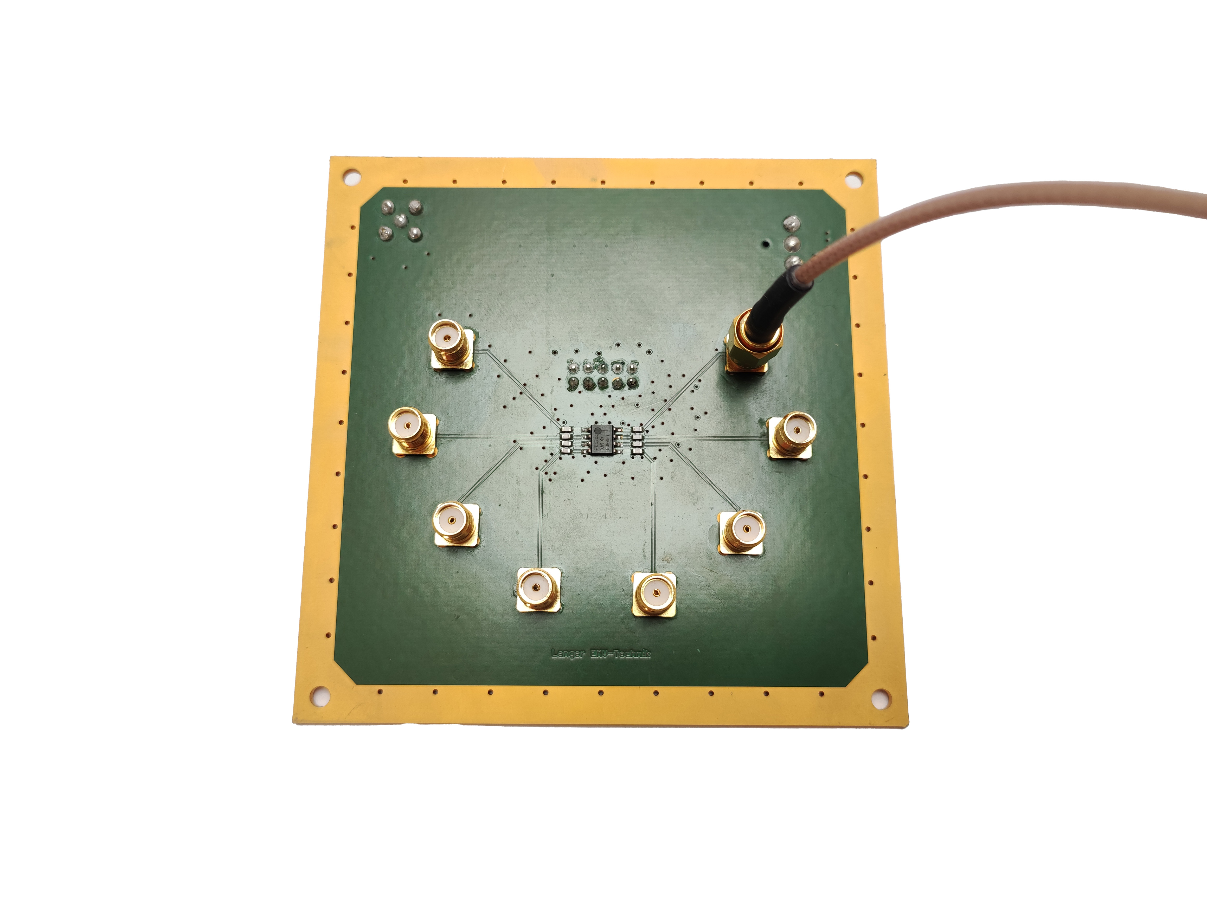
For DPI tests involving ICs with more than 100 pins, the design of the test PCB quickly becomes complex and confusing. In this case, either only a small number of relevant pins are tested, or several test PCBs are designed, each targeting different pin groups.
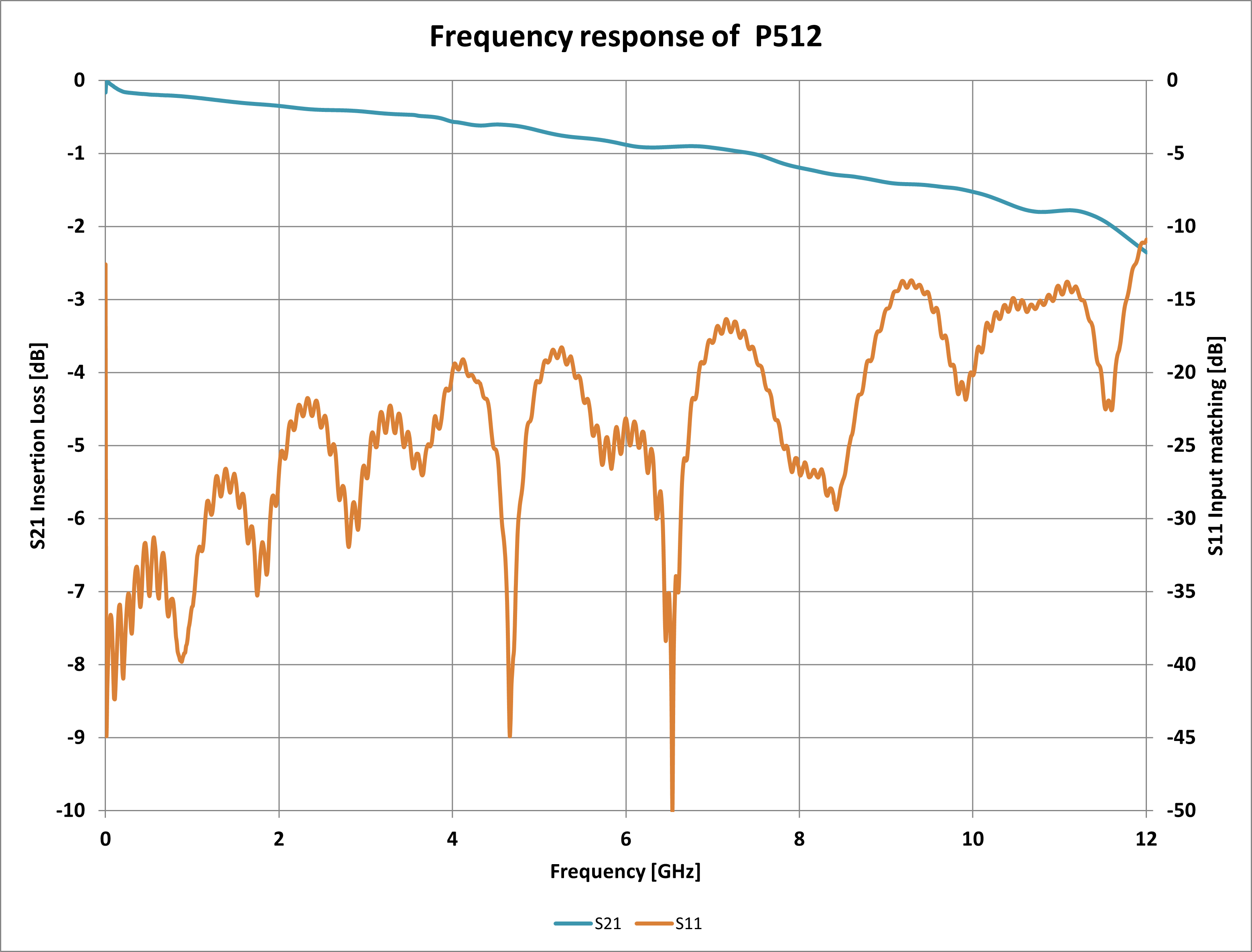
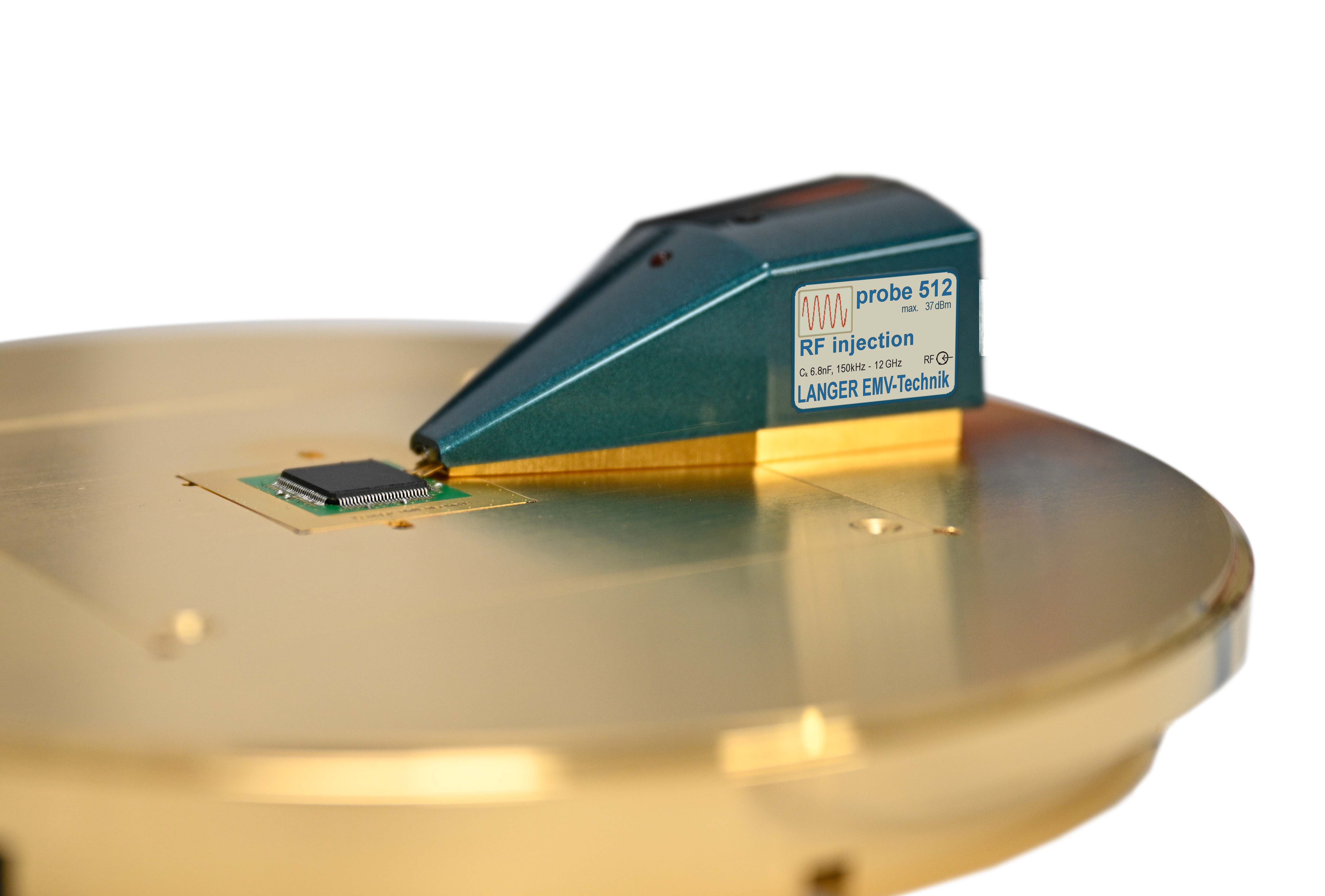
The new product from Langer EMV-Technik, the P512 probe, is capable of coupling RF power of up to 12 GHz into IC pins. A special contact system with a large-area ground connection is used for this purpose. The probe's cut-off frequency of 12 GHz was measured using an IC stripline within the ground system.
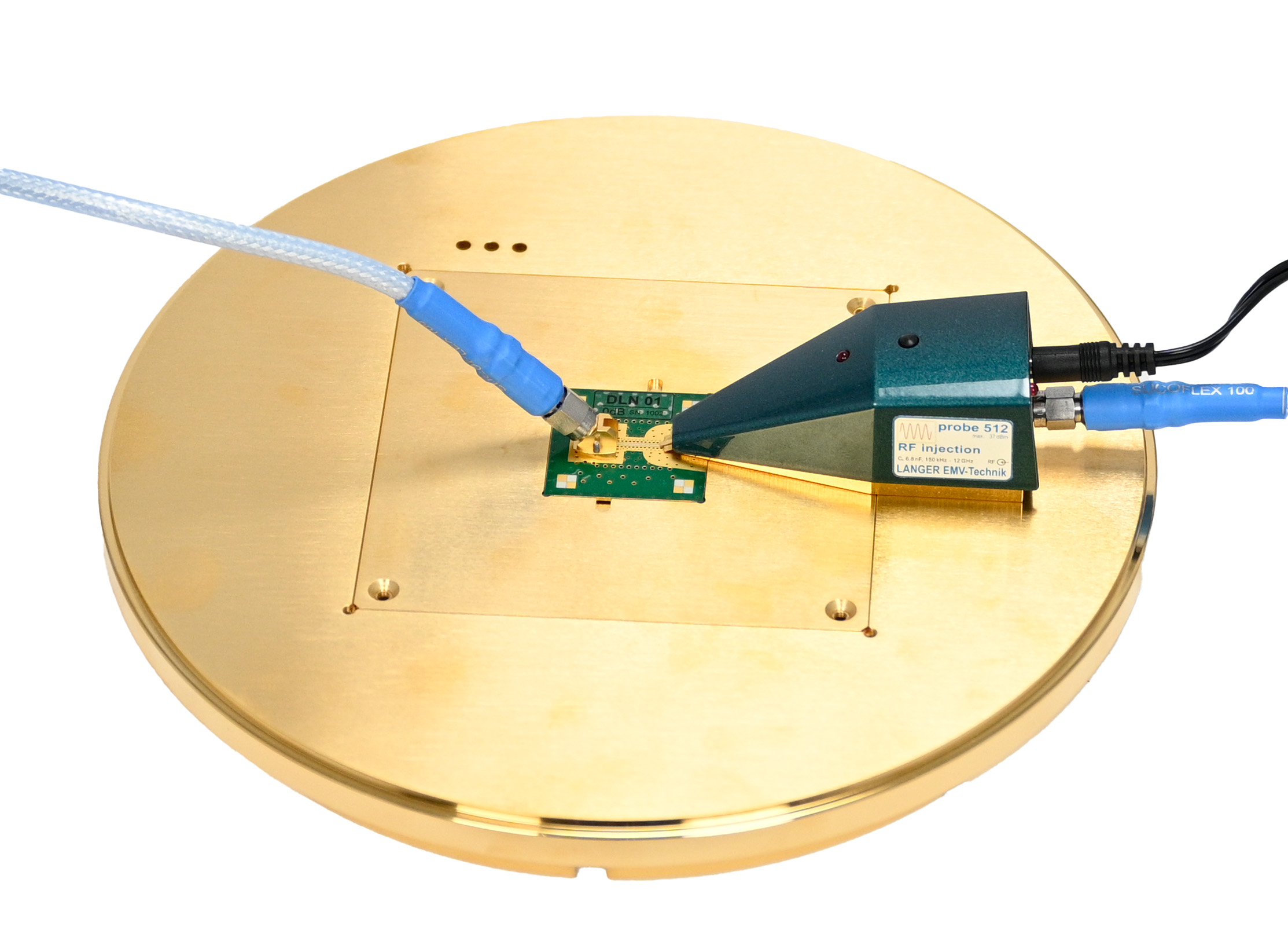
The main advantage of using the P512 is the frequency range up to 12 GHz for the coupling of RF power. ICs manufactured using flip-chip technology and housed in a BGA package are particularly susceptible in this higher frequency range. Further advantages result from the special design of the probe in combination with the ground system included in the set. The IC pins no longer have to be contacted separately via the SMA connector of the respective pin in order to couple in RF power; instead, the probe itself is connected to the power amplifier with the SMA connector on the back of the probe. The pins are then contacted using the tip of the probe, which can be freely positioned on each pin of the IC. This eliminates the need to switch between testing two pins and makes it possible in principle to automate the measurement. The 6.8 nF coupling capacitance is located inside the probe and no longer needs to be taken into account when designing the test PCB.
Use as RF probe head
The P512 can also be used as an RF probe for measuring high-frequency signals up to 12 GHz. The measurement takes place in the same ground system as the coupling. The advantage of freely contacting of pins as already mentioned for coupling, is therefore retained. Due to the ground contact of the sample directly next to the measuring tip, potential coupling loops remain minimal, which leads to reduced feedback in the measurement. When measuring high-frequency useful signals, the signal may be capacitively loaded and distorted by the 6.8 nF. In such a case, the internal coupling capacitance of the probe can be adjusted to any value in the pF range.
Contact
For further information, please contact sales@langer-emv.de.