
Manual
ESD magnetic field injection set
ESD magnetic field source P1202-2
1 ESD field source for magnetic fields
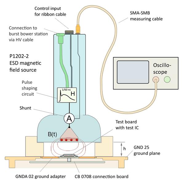
The P1202-2 probe is a field source. The field source allows the user to couple defined and reproducible ESD fields to IC housings (Figure 3).
Modules and devices are tested according to the ESD standard IEC 61000-4-2. During this test, the ESD generator is discharged onto the device.
Electric and magnetic fields develop during the ESD discharge. These fields may penetrate the device under test and its electronic system and even penetrate IC housings and result in interference in the ICs. Therefore, field coupled interference (inductive / capacitive) are also a source of interference with ICs besides the conductive coupling.1.
The field source P1202-2’s design is based on how the ESD (IEC 61000-4-2) is coupled to the IC through fields.
The shape of the fields in the IC's placement area is mainly determined by the inner metallic structure (layout) of the printed circuit board. Printed circuit boards usually contain continuous copper layers which shape the fields.
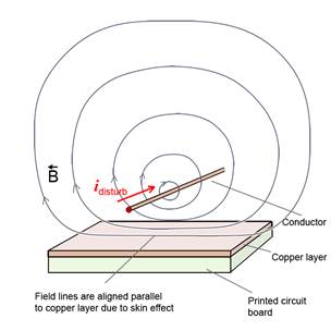
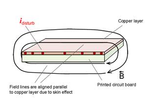
Magnetic fields are aligned parallel to the printed circuit board due to the flux displacement effect (associated with the skin effect) (Figure 1 and Figure 2). These directional fields affect the ICs in the IC placement area. The field lines align parallel to the IC housing. The field sources have to simulate this magnetic field orientation (Figure 5).
1 Conducted EFT/burst tests of ICs are performed with the P200 and P300 probe families from Langer EMV-Technik GmbH
Field lines that are perpendicular to the IC housing only occur in special cases. The BS 04 DB-h and BS 05 DB-h field sources in the "H3 set of burst field sources for generators according to the standard EN 61000-4-4" from Langer EMV-Technik GmbH can be used to generate these fields.
Electric fields are always emitted orthogonally from metallic surfaces. Hence, it follows that the copper layers inside a printed circuit board are responsible for this orthogonal field orientation. E-field sources have to simulate this orthogonal field orientation to the printed circuit board and test IC. Local fields can be generated with the ES 05 D-h field source ("H3 set of burst field sources for generators according to the standard EN 61000-4-4" from Langer EMV-Technik GmbH).
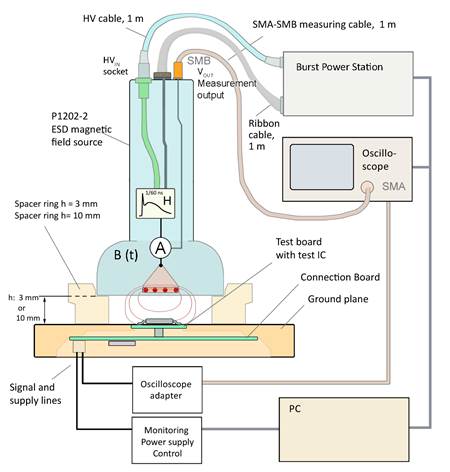
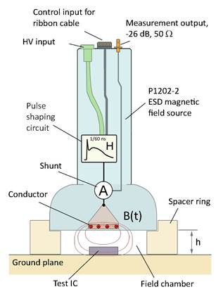
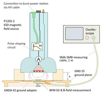
The field source must be operated with the BPS 203 burst power station. The BPS 203 burst power station controls and supplies the P1202-2 field source (1.3 Set-up of the test bench / system set-up). The variation over time of the field source's field is equal to that of an ESD generator's discharge pulse current. The waveform of the discharge current pulse is defined in the standard IEC 61000-4-2 (Figure 6).
The field source can only be operated in conjunction with the BPS 203 burst power station!
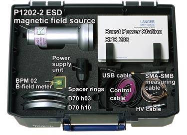
The test equipment comprises the P1202-2 field source of the probe set, the ICE1 test environment and measuring instruments.
2GNDA 02 ground adapter, GND 25 ground plane and CB 0708 connection board are included in the ICE1 IC test environment. www.langer-emv.de The test board is described in the "IC test instruction manual", www.langer-emv.de.
1.1 Design of the P1202-2 magnetic field source
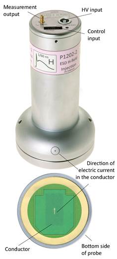
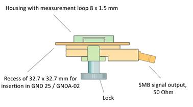
The field source has an HV input (Fischer socket, D103A023) on its top to connect an HV cable. A high voltage is supplied from the BPS 203 burst power station to the field source via this HV cable. The HV input is connected to the pulse shaper circuit inside the field source. The pulse shaping circuit uses this voltage to produce the discharge current. The waveform of the discharge current corresponds to the waveform of the discharge current according to the standard IEC 61000-4-2 (Figure 6). The discharge current from the pulse shaper circuit is supplied to the field source's electric conductor (Figure 4).
The electric conductor is at the bottom of the field source. It uses the discharge current to generate the magnetic ESD test field which is emitted from the bottom of the field source. A shunt is located in the electric conductor of the field source to measure the discharge current (iP) (Figure 5).
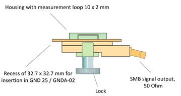
The output voltage of the shunt can be measured through the field source's measurement output. The measurement output is terminated with 50 Ω in the field source. A field chamber encloses the magnetic field which is generated by the electric conductor in the field source. The field cell comprises the bottom of the field source, the spacer ring and the ground plane. The test IC is located inside the field cell. It is mounted on the test board (Figure 3). The test board is inserted into the ground plane.
The pulse shaper circuit is connected to the BPS 203 burst power station via the “control” socket (Figure 5, Figure 3) and ribbon cable. The BPS 203 burst power station controls the pulse shaper circuit via this connection.
1.2 Function of the P1202-2 magnetic field source
The BPS 203 burst power station is connected to the HV input via the HV cable (Figure 3). The HV current flows from the BPS 203 burst power station through the HV cable to the HV input which is connected to the pulse shaper circuit. The pulse shaping circuit uses this voltage to produce the discharge current. The waveform of the discharge current (Figure 6). corresponds with IEC 61000-4-2. The discharge current of the P1202-2 field source is 10.5 times higher than the current specified in the standard IEC 61000-4-2 with the same high voltage.
The discharge current generates the magnetic field B around the electric conductor in the field cell which is applied to the test IC during the test (Figure 5).
The strength of the magnetic field and the voltage induced in the test IC can be determined in the following ways:
- Table 4 Disturbances of the P1202-2 magnetic field source depending on the high voltage UP
- Calculation of the probe curren IP from the high voltage UP
- Measurement of the current iP(t) at the shunt of the P1202-2 field source
- Calculation of the magnetic flux in the area of the test IC from the current iP and the probe constant K1 Table 4 of the P1202-2 field source
- Calculation of the voltage uIC im Test-IC aus dem Strom IP and the probe constant K2 of the field source Table 3
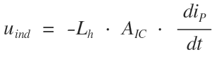
- Calculation of the voltage uICinduced in the test IC from the coupling inductance Lh between the electric conductor and test IC and fromP/dt
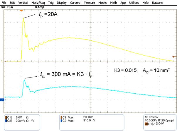
- Calculation of the current iIC transferred to the IC on the basis of the probe current iP of the P1202-2 field source and the probe constant K3 (coupling factor, see Figure 22)
1.2.1 Determination of the current iP in the electric conductor of the field source
The probe current iP of the field source is required to calculate the magnetic field. There are two ways to determine the current iP.
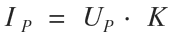
1. Calculation of IP from the set high voltage UP
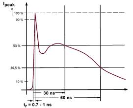
The parameters of the discharge current (first discharge current peak, current at 30 ns, current at 60 ns) are calculated with the following equations:
 | Eq 1 |
| KFirst discharge current peak | 36 A/ kV |
| K30ns | 19.2 A/ kV |
| K60ns | 9.6 A/kV |
| Table 1 Current constants | |
The aforementioned equation (Eq 1) and the current constants (Table 1) allow the calculation of the current IP, of the P1202-2 field source, in the electric conductor from the high voltage UP. The variation of the current iP over time can be measured with the shunt and an oscilloscope.
2. Measurement of the current iP
The current ip is measured in the field source with a shunt (0.1 Ohm). The measurement output is matched to 50 Ohm. The oscilloscope's input has to be set to 50 Ohm to obtain correct values during the measurement. The attenuator is set to 26 dB (x20) in the vertical menu of the oscilloscope. Make sure that the measurement signal does not exceed the oscilloscope's maximum permissible input voltage. An external attenuator should be used if necessary.
The current measurement is much more precise than the calculation from the voltage set at the BPS 203 burst power station.
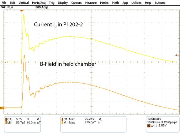
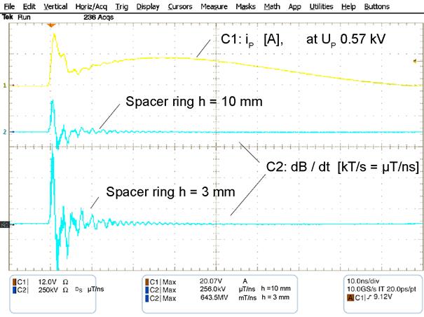
Figure 8 shows the current (iP) and the flux density (B) of the P1202-2 field source as a function of time; and the proportionality of the probe current iP and flux density B variation over time in the field cell.
1.2.2 Disturbance mechanism of the magnetic field B
A magnetic field is generated in the field chamber of the field source when a current flows in the electric conductor of the field source. The vortex magnetic field penetrates the test IC (Figure 5).
The test IC contains conductor loops (Figure 9). The largest conductor loops of the test IC are formed by the pins, bond wires, lead frames and the die. AIC is the cross-section of a current loop. The vortex magnetic field B penetrates the conductor loop and induces the disturbance voltage uindin this loop.
This induced disturbance voltage uind can have a direct effect on signals inside the IC3 or drive a disturbance current through the IC. The disturbance current can affect the Vdd / Vss supply systems and trigger faults and/or generate voltage differences between different circuit sections.
3 Dipl. Ing. Gunter Griessbach und Dipl. Ing. Gunter Langer, „Integrierte Schaltkreise (IC) sind heute die EMV-Schwachstellen elektronischer Geräte.“ Elektronik, 2014
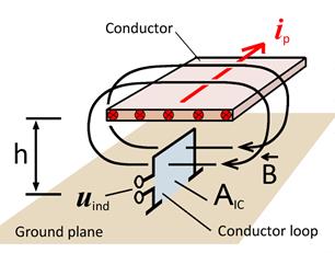
The open IC loop which is shown in Figure 9 is closed by the resistance RIC (not shown in the figure). The resistance RIC(not shown in the figure). The resistance RIC is formed by pull-up/pull-down resistance, driver resistance and the IC's internal resistance. The ohmic resistance of the line network establishes the resistance in supply loops (Figure 22).
The magnetic field's effect on the IC loop is best if the magnetic field B penetrates the loop at a 90 degree angle. The loops inside the IC may have different orientations. It is thus important that the magnetic field's direction can be changed so that all critical loops can be identified. The field source can be rotated in the spacer ring for this purpose. The direction of the magnetic field that penetrates the test IC can thus be changed gradually in all directions from 0-360°. The different settings therefore allow the application of a maximum field to the loops with different orientations inside the IC via the pin connections or in the die. Furthermore, the orientation of critical loops in the IC can be determined.
The level of the voltage induced in the device under test and its resulting interference effect depend on parameters such as:
- Value set for the high voltage (UP)
- Size of the conductor loop in the IC (AIC)
- Distance (h) from the ground plane to the electric conductor of the field source
- Angle between the electric conductor and the conductor loop
1.2.3 Calculation of the magnetic field B
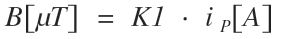
Der magnetische Fluss im Bereich des Test-ICs lässt sich mit folgender Gleichung berechnen:
 | Eq 2 |
Whereby K1 is a probe constant which depends on the metallic structure of the field cell and electric conductor (Figure 5).The field chamber can be set to two different heights with the spacer rings (10 mm, 3 mm). All other dimensions of the field chamber and electric conductor are identical for all field sources. Consequently, there are two probe constants K1 of the field sources which can be assigned to the heights of 10 mm and 3 mm (Table 3).
These constants K1 are identical for all magnetic field sources (burst, ESD, RF) of the IC test system from Langer EMV-Technik GmbH.
The magnetic flux density B in the area of the test IC can also be found in Table 4
1.2.4 Measurement of the magnetic field B
The BFM 02-B4 B-field meter can be used to measure the magnetic flux density B in the field chamber at the test IC location (Figure 10). The B-field meter is inserted into the ground adapter instead of the test IC. BFM 02-B B-field meter fits into the GNDA 025.ground adapter and has to be inserted into the GND 256 ground plane for the measurement (see ICE1 test environment user manual).
The SMB output of the B-field meter is connected to the input of the oscilloscope via the 50 Ohm SMA-SMB measuring cable (Figure 11). The measurement output is matched to 50 Ohm. The oscilloscope's input has to be set to 50 Ohm to obtain correct values during the measurement. The attenuator value shown on the B-field meter is entered in the vertical menu of the oscilloscope. The flux density is displayed on the oscilloscope in µT (or pVs/mm2) with this attenuator value.
Ensure that the measurement signal does not exceed the oscilloscope's maximum input voltage. An external attenuator should be used if necessary. A pre-amplifier can be used if the signal is too weak (PA 303, 30 dB, www.langer-emv.com).
4The BFM 02-B is not included in the probe set's scope of delivery; can be ordered separately.
5The GNDA 02 is included in the ICE1's scope of delivery. www.langer-emv.com
6The GND 25 is included in the ICE1's scope of delivery. www.langer-emv.com
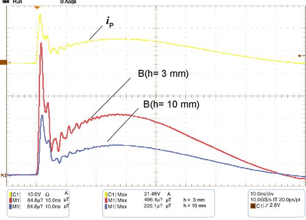
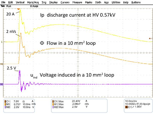
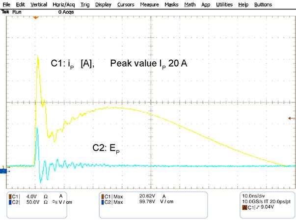
Figure 12 shows the flux density curves for a high voltage UP = 0.57 kV and a current iP = 20 A for a 3 mm and 10 mm spacer ring.
1.2.5 Measurement of the induction dB/dt
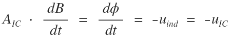
The BPM 02 Ḃ-field meter can be used to measure the dB /dt = Ḃ-value in the field chamber at the test IC location (Figure 13).The Φ / dt flux variation over time in the IC conductor loop and the voltage uind induced in the IC can be calculated on the basis of dB / dt (Ḃ) and the cross-section AIC of the IC conductor loop:
 | Eq 3 |
whereby Φ is the magnetic flux which penetrates the IC conductor loop.
The BPM 02 Ḃ-field meter is inserted into the ground adapter instead of the test IC. The BPM 02 Ḃ-field meter fits into the GNDA 027 ground adapter and has to be inserted into the GND 25 ground plane for the measurement (see ICE1 IC test environment user manual).
7The GNDA 02 is part of the ICE1.
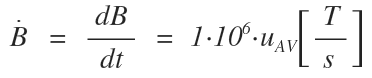
Der SMB-Ausgang des Ḃ-Feldmessers wird mit dem 50 Ohm SMA-SMB Messkabel mit dem Eingang des Oszilloskops verbunden (Figure 15). Der Messausgang ist auf 50 Ohm angepasst. Um korrekte Messwerte zu erhalten, muss der Eingang des Oszilloskops auf 50 Ohm eingestellt werden. Die im Oszilloskop anstehende Spannung uAVwird für den Ḃ-Feldmesser BPM 02 mit folgender Gleichung in Ḃ umgerechnet:
 | Eq 4 |
The attenuator value 1 • 106 has to be entered in the vertical menu of the oscilloscope Figure 14.
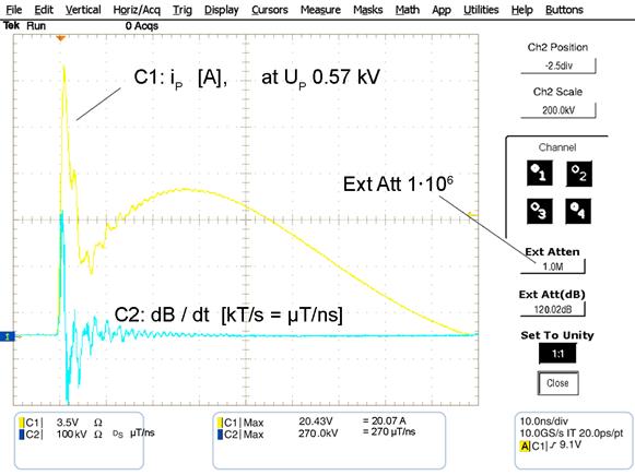
If a Ḃ-field meter with another attenuator value is used, this has to be entered in the vertical menu of the oscilloscope. Ḃ Ḃ is displayed on the oscilloscope in T/s with the respective attenuator value. Ḃ is displayed in V (Volt) or kV if the unit of measurement is not changed from V (Volt) to T or µT in the channel of the oscilloscope (Figure 14). Ḃ = 270 kV is displayed, for example. The value displayed in this form has to be converted using the "Meter-Kilogram-Second-Ampere system" (MKSA system) to display the value in T/s. T/s can be resolved in Vs/m2 s by converting k from kV to µ/n. µVs/ m2 ns = µT/ns is now the channel's unit of measurement.
Ensure that the measurement signal does not exceed the oscilloscope's maximum input voltage.
An external attenuator should be used if necessary. A pre-amplifier can be used if the signal is too weak (PA 303, 30 dB, www.langer-emv.com).
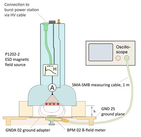
Figure 16 shows Ḃ as a function of time for an ESD generator voltage UVG = 0.57 kV and a current iP = 20for a spacer ring of 3 mm and 10 mm.
The voltage which is induced in an IC can be determined if the effective cross-section AICof the IC loop is known.
 | Eq 5 |
uind can be calculated from Ḃ with a mathematical function in the oscilloscope (Figure 17).
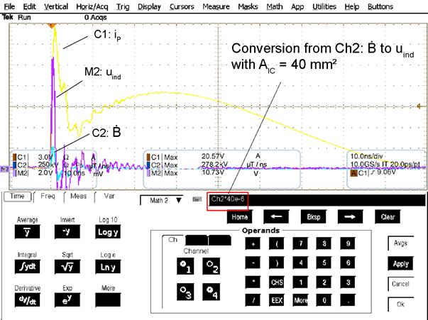
The largest IC conductor loops are formed by the pins, bond wires, lead frames and the die. A voltage of 10.7 V is induced in a loop of 2 mm by 20 mm at an ESD current of 20 A and a spacer ring height of h = 10 mm.
Ḃas a function of time can be converted to the flux density B by integration.
 | Eq 6 |
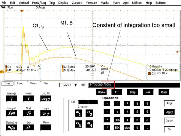
whereby C is the constant of integration. The integration can be performed in the oscilloscope (Figure 18) The unit of measurement of the result calculated in the oscilloscope is T.
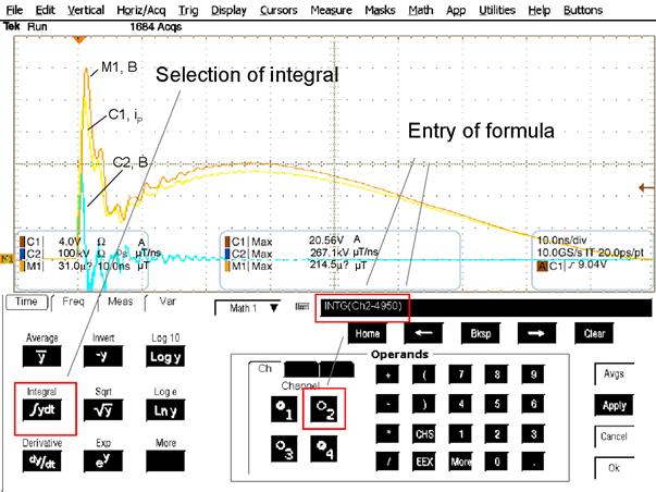
The value of the constant of integration C has to be entered in the equation of the oscilloscope by hand. The final value of the constant of integration is determined by iteration. 0, for example, can be used as the initial value. If the value of the constant of integration C is too low, the measured curve will drop relative to the expected variation (Figure 19). The expected variation is proportional to the variation of the current iP in the electric conductor (Figure 18). The constant of integration C has to be increased if the measured curve drops instead. If the measured curve rises, however, the value of the constant of integration C is too large (Figure 19).and then has to be reduced by hand. The value of the constant of integration has to be gradually adjusted by hand until the variation over time for C2: Ḃ is proportional to that of the current C1: iP (Figure 18).

If the attenuator value (Ch2) that has been entered in the oscilloscope converts the measured signal UAV to T / ns, AIC has to be entered in m2 in the equation of the oscilloscope. The unit of measurement of the result displayed on the oscilloscope is then T.
If the attenuator value which has been entered in the oscilloscope converts the measured signal UAV to in mV/mm2 AIC in mm2 in the equation of the oscilloscope. The unit of measurement of the result displayed by the oscilloscope is then Vs/mm2.
1.2.6 Mechanism of inductive coupling from the P1202-2 field source to the test IC
Regarding inductive coupling it is important to distinguish between current coupling and voltage coupling (Figure 21 and Figure 22).
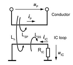
The current iP in the electric conductor generates a vortex magnetic field. The share of the vortex magnetic field which penetrates the IC loop is assigned to the principal inductance Lh The principal inductance Lh mediates between the current iP of the field source and the voltage uIC which is induced in the IC loop.
 | Eq 7 |
The IC loop has the self-inductance Lss. The connection between P1202-2 and the electric conductor shown in Figure 21 can be transferred to a lumped-element transformer equivalent circuit (Figure 22).
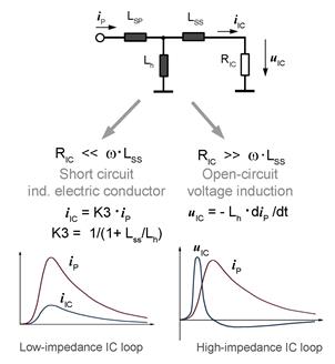
Distinction of cases:
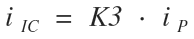
1. Current coupling
The circuit operates under short-circuit conditions if << ω LSS The inductances Lh and LSS form a current divider. The currents are divided at the ratio Lh / LSS independent of the frequency (reduced from LSS >> Lh: 1/(1+LSS/Lh) = Lh/LSS). The waveform of the current pulse in the IC is thus equal to that of the discharge current in the electric conductor of the field source. This means that a current pulse iIC 1/60 ns flows in the IC. The peak value is attenuated by the coupling factor K3 (Figure 22) RIC must be in the range of 0.1 Ohm so as to transfer all frequency components of the discharge current. This is implemented in Vdd / Vss loops.
2. Voltage coupling
The circuit operates like a voltage transformer under open-circuit conditions if RIC >> ω LSS. The voltage induced on the inductance Lh is present in the IC (open-circuit voltage). It changes depending on the frequency according to the law of induction.
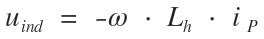 | Eq 8 |
The induced voltage uind is proportional to the frequency of the current iP This is particularly important for ESD coupling as the current consists of higher frequency parts than the EFT/Burst current.
1.2.7 Current coupling to the IC
The Lh / L s ratio (reduced from LSS >> Lh: 1/(1+LSS/Lh) = Lh/LSS) determines the coupling of current to an IC loop (Figure 22). The ratio remains practically unchanged if the width of a conductor loop is changed. Changing the loop's height and line diameter would result in a change of Lss nAs a result, Lss does not clearly depend on the loop area AIC. A normalisation could only be performed under the aforementioned conditions and has not been performed in this case.
The resistance RIC essentially determines the effectiveness of current coupling. Current coupling is effective for supply loops due to their low resistance. Lh can be determined on the basis of the inductance per unit length L’ and AIC for calculations Lss has to be determined on the basis of the IC design.
 | Eq 9 |
K3 has been determined by measurements in Figure 23.
1.2.8 Voltage coupling to the IC
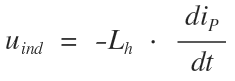
The electric conductor of the field source is coupled inductively to the conductor loop in the test IC. The coupling effect is described by the law of induction,
 | Eq 10 |
Whereby the inductance Lh is the measure of coupling between the electric conductor and the loop of the test IC.
The specific inductance Lh' is the ratio between the inductance Lh and the effective surface area of the test-IC loop.
This specific inductance Lh' is a constant for the field chamber and is listed in Table 3 for a field chamber height h of 3 mm and 10 mm. The induced voltage is calculated with the equation,
 | Eq 11 |
whereby Lh' is the specific inductance of the field chamber at the test IC location. AIC is the effective cross-section of the test IC loop. The cross-sections AIC of the loops in the test IC can be determined on the basis of its design. The voltage which is induced in the loop of the test IC can be calculated from this value, the inductance per unit length and the current differential diP / dt. These values can be used for a simulation on the IC.
diP / dt for ESD can be roughly calculated from the rise time of the pulse Δt and the peak value of the current ΔiP of the first discharge peak,
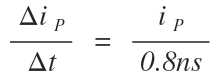 | Eq 12 |
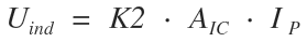
with K2 = Lh' / Δt and uind = - Lh' • AIC • diP / dt it is possible to calculate the maximum voltage (depending on the first discharge peak).
 | Eq 13 |
The values of K2 can be found in Table 3.
diP / dt can also be measured with an oscilloscope according to the measuring method 1.2.4.
Im Figure 24 shows the variations of the induced voltages over time for a test conductor loop of AIC = 10 mm2 dargestellt.
The induced voltage can be calculated directly from the flux density in the area of the test IC.
 | Eq 14 |
The equation establishes a direct relationship between the magnetic field B and the induced voltage
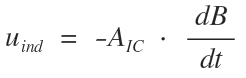
1.2.9 E-field suppression of the ESD magnetic field sources
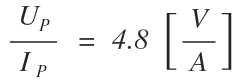
A weak electric field EP.is generated in the field chamber of the P1202-2 field sources as a parasitic effect when a magnetic field is generated. The electric field depends linearly on the supply current IP and the spacer ring height h. Figure 25 shows the electric field as a function of time. It corresponds to the first derivative of the current on account of the inductive voltage drop in the electric conductors of the field source, amongst other things.
The associated electric voltage UP to ground is independent of the height of the spacer ring:
 | Eq 15 |
(P1202-2, h = 10 Figure 25)
However the electric field in the area of the test-IC is dependant from the height of the spacer ring (given a constant voltage Up (Table 6).
1.3 Set-up of the test bench / system set-up
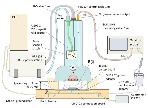
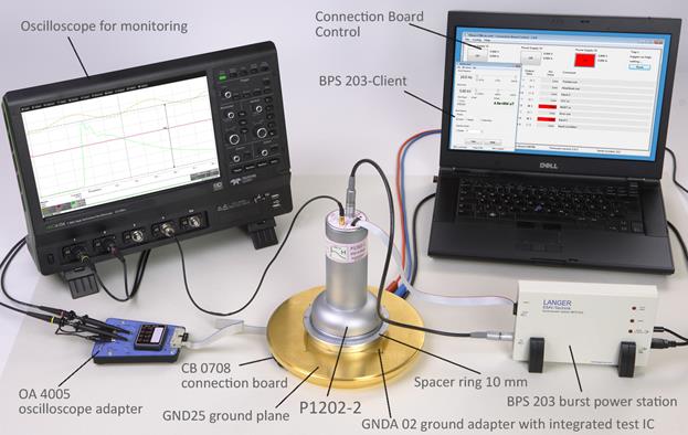
Im Figure 26 shows the set-up of the test bench with the ICE1 test environment (Table 2) and the P1202-2 field source. The BPS 203 burst power station generates the high voltage required to operate the P1202-2 field source.
The HV port of the BPS 203 burst power station is connected to the HVIN input of the field source via the HV FI FI 1 m cable. In addition, the Control output of the field source is connected to the Probe port of the BPS 203 via the control cable (FBK 12P 1 m). The BPS 203 is connected to a PC via the USB B cable. The BPS 203-Client software and Windows drivers are installed on the PC (BPS 203 user manual). The BPS 203 is controlled from a PC via its USB interface.
The ESD magnetic field is generated in the P1202-2 field source from the high voltage which is supplied by the BPS 203. The ESD magnetic field acts on the housing of the test IC inside the field chamber. The test IC is mounted on a test board. Manufacturing the test board is described in Chapter 3 of the Guide line IC EFT immunity (mail@langer-emv.de). The test board is inserted into the GND 25 ground plane and connected to the CB 0708 connection board via a plug connector (Figure 26).
The ground plane and connection board are components of the ICE1 IC test environment (ICE1 user manual).
Two different spacer rings are included in the scope of delivery. The spacer rings have a height of 3 mm and 10 mm respectively. The height of the field source can be defined by selecting the respective spacer. The 3 mm spacer ring leads to a higher field strength in the field chamber but the electrode or the electric conductor is closer to the test IC.
The proximity to the test IC causes a stronger field distortion with 3 mm than with 10 mm. The measuring accuracy is thus higher when using the 10 mm spacer ring. The 3 mm spacer ring can be used if the field strength is not sufficient to interfere with the test IC at the maximum generator voltage. When using the 3 mm instead of the 10 mm spacer, the magnetic flux density is increased by the factor 2 (neglecting the test IC interaction).
When using the 3 mm instead of the 10 mm spacer, the magnetic flux density is increased by the factor 2 (neglecting the test IC interaction).
The chosen spacer ring is mounted on the GND 25 ground plane (Figure 26). The P1202-2 field source is then inserted into the recess of the spacer ring. The field source can be rotated in the spacer ring. The direction of the magnetic field that penetrates the test IC can thus be changed gradually in all directions from 0-360°.
The OA 4005 oscilloscope adapter and the CB 0708 connection board can be used to evaluate signals from the test IC. The CB 0708 connection board and a control unit can be used to control the test IC. The ICE1 user manual provides information on how to use and wire these components. Figure 27 shows the set-up of a practical test bench.
The devices listed in the table are described in their respective instruction manuals:
| Task | Instruction manual |
|---|---|
|
|
|
|
|
|
|
|
| Table 2 Documentation | |
1.4 Performance of the test
There are two ways of using the test bench:
1. Manual control of the test bench
The BPS 203 and thus the P1202-2 are controlled via the user interface of the BPS 203-Client software. The pulse parameters are set on the software user interface. The monitoring signals (sources: oscilloscope, oscilloscope adapter, connection board or proprietary solution of the user) have to be evaluated by the user.
2. Automated or semi-automated test bench
Since an automated test bench depends on the type of test IC monitoring signals, it is up to the user to develop automated or semi-automated solutions (advice from Langer EMV-Technik GmbH, mail@langer-emv.de).
The test bench PC must allow an evaluation of the monitoring signals of the test IC. The sources of the monitoring signals are the oscilloscope in conjunction with the OA 4005 oscilloscope adapter and the connection board or proprietary solutions of the user.
BPS 203 and Connection board CB 0708 can be controlled remotely by a DLL (included in scope of delivery) via LABView or Vee (Keysight). Please refer to the BPS 203 user manual and ICE1 user manual (CB 0708 connection board for a description).
BPS 203 features an external trigger input. With this input the user can trigger a pulse at the P1202-2 with a provided logic signal.
1.4.1 Test procedure
The test IC is tested in operation (this may require a customized firmware, see “Guideline IC-Test”). In general, the disturbance (ESD – magnetic field) is gradually increased in the course of the test. The pulse repetition frequency is set in the BPS 203 client software. A defined number of pulses or a test duration can be set.
The period over which the disturbance is applied to the test IC depends on the probability of disturbing crucial signals in the test IC. Experience has shown that test periods of approx. 1 minute are sufficient in most cases. Longer test periods are needed if the probability of disturbing a critical signal / operating state of the IC under test is low. The test periods also depend on the safety demands in terms of the subsequent IC use.
The procedure is described in Chapter 3 of the Guide line IC EFT immunity (scope of delivery ICE1). In general, the P1202-2 should be switched off if the test IC signals any interference via its monitoring signals (monitoring OA 4005 oscilloscope adapter, LEDs of the GND 25 ground plane, CB 0708 connection board with transmission to the PC, user solutions). In particular cases, the voltage can be further increased until other faults occur (monitoring OA 4005 oscilloscope adapter, LEDs of the GND 25 ground plane, CB 0708 connection board with transmission to the PC, user solutions). The IC can be destroyed in this case. The risk can be reduced by monitoring or limiting the IC's power supply (connection board). The supply voltage can be interrupted in the case of a fault by an emergency shut-off function. The emergency shut-off can be triggered manually via a control unit or a proprietary solution of the user (automatically from the PC).
The disturbance field is generated in the field chamber of the field source when operating the test bench. Make sure that the field chamber is not opened during the test for safety reasons. The field source may only be operated with the field chamber closed by the spacer ring and ground plane.
1.4.2 Verifying the waveform of the test pulse
The waveform of the test pulse has to be verified prior to every major measuring job. Provided the waveform does not deviate from the given parameters, the field source only has to be calibrated every two years by Langer EMV-Technik GmbH.
The chapters 1.2.4 and 1.2.5 describe how to verify the waveform.
2 Safety instructions
This product meets the requirements of the following directives of the European Union: 2004/108/EC (EMC directive) and 2006/95/EC (low-voltage directive).Please observe the following safety instructions when using a product from LANGER EMV Technik GmbH to protect yourself against the risk of electric shocks or injuries.
Read and follow the operating instructions and keep them in a safe place for later consultation. The device may only be used by personnel who are qualified in the field of EMC and who are fit to work under the influence of disturbance voltages and (electric and magnetic) EFT/burst/ESD fields.
- Observe the operating and safety instructions for all devices used in the set-up.
- Never use any damaged or defective devices.
- Carry out a visual check before using a measurement set-up with a Langer EMV-Technik GmbH product. Replace any damaged connecting cables before starting the product.
- Never leave a product from Langer EMV-Technik GmbH unattended whilst this is in operation.
- The Langer EMV-Technik GmbH product may only be used for its intended purpose. Any other use is forbidden.
- People with a pace-maker are not allowed to work with this device.
- The test set-up should always be operated via a filtered power supply.
- Attention! Functional near fields and interference emissions may occur when the field source is operated. The user is responsible for taking appropriate precautions to prevent any interference to the correct function of products outside the operational EMC environment (in particular through interference emissions).
This can be achieved by:- observing an appropriate safety distance,
- use of shielded or shielding rooms.
We cannot assume any liability for damage due to improper use.
- The disturbances that are injected into the modules can destroy the device under test (latch-up) if their intensity is too high. Protect the device under test by:
- connecting a protective resistor in the IC's incoming power supply
- increasing the disturbance gradually and stopping when a functional fault occurs,
- interrupting the power supply to the device under test in the event of a latch-up.
Attention! Make sure that internal functional faults are visible from outside. The device under test may be destroyed due to an increase in the injection intensity if the faults are not visible from outside. Take the following precautions if necessary:
- monitor the representative signals in the device under test,
- special test software,
- visible reaction of the device under test to inputs (reaction test of the device under test).
We cannot assume any liability for the destruction of devices under test!
3 Warranty
Langer EMV-Technik GmbH will remedy any fault due to defective material or defective manufacture, either by repair or by delivery of spare parts, during the statutory warranty period.
This warranty is only granted on condition that:
- the information and instructions in the user manual have been observed.
The warranty will be forfeited if:
- an unauthorized repair is performed on the product,
- the product is modified,
- the product is not used for its intended purpose.
Scope of delivery
Link to the scope of delivery